Stephen Hawking once said, “Without imperfection, neither you nor I would exist.” In the world of electronics, imperfections aren’t just inevitable — they’re essential. From doped silicon chips to finely tuned sensors, defects often determine how a material behaves.
Now, researchers from the Indian Institute of Science (IISc) Bengaluru, GITAM University Bengaluru, and the National Institute for Materials Science, Japan, have shown that tiny flaws in molybdenum disulfide (MoS₂) — a two-dimensional semiconductor — could be the key to building better electronic and optoelectronic devices.
Why MoS₂?
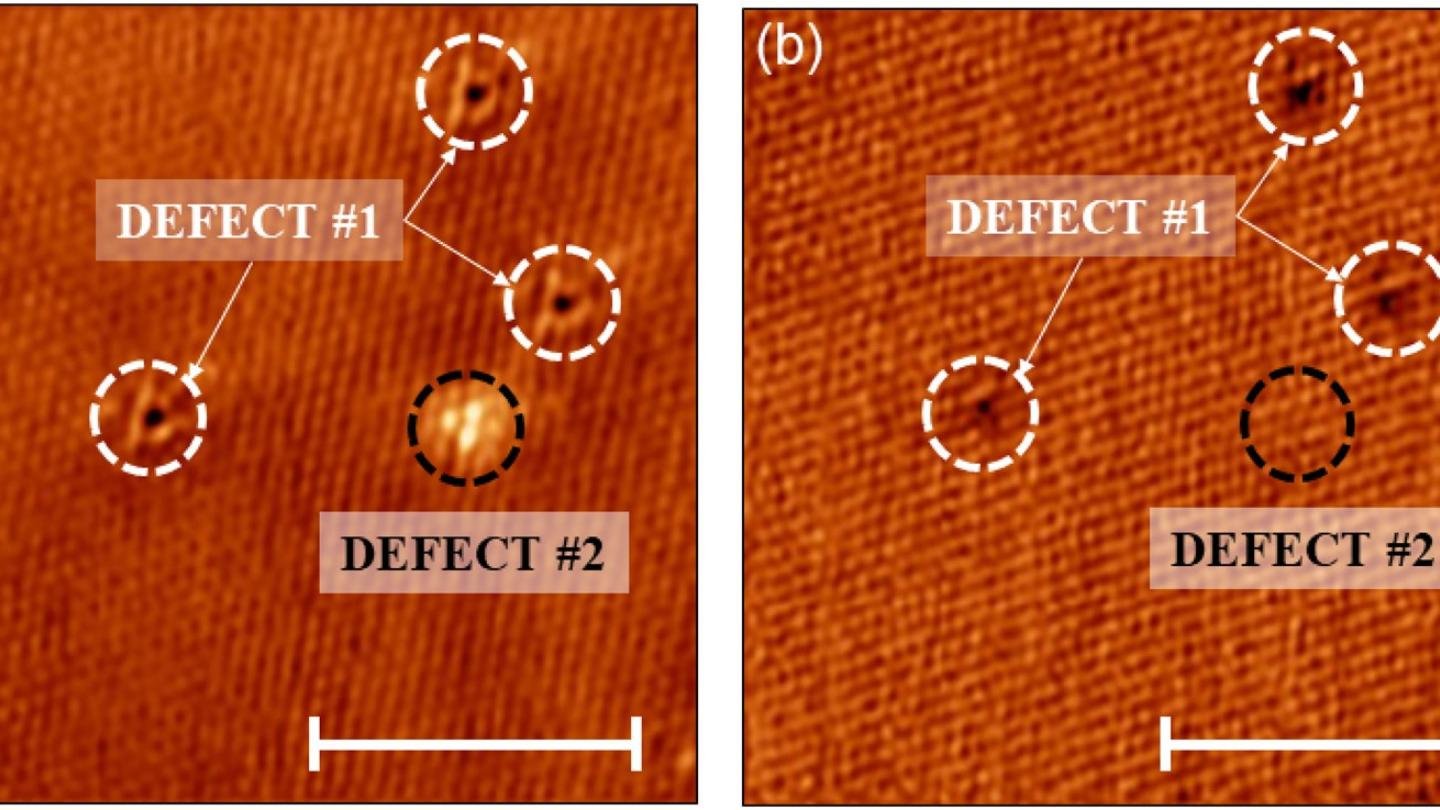
MoS₂ is made of layers of sulfur–molybdenum–sulfur atoms arranged in a hexagonal pattern. When exfoliated into ultra-thin sheets, it offers promising properties for next-gen transistors and sensors. But like all real-world materials, it comes with defects — and instead of eliminating them, the team decided to study and harness them.
The Experiment
The researchers placed a single layer of MoS₂ on an ultra-clean, insulating surface of hexagonal boron nitride (hBN). They then built a field-effect transistor (FET) from this setup to study how electrons moved through the material under different temperatures and voltages.
At low temperatures, electrons didn’t flow freely; instead, they “hopped” between defect-induced localised states. By analysing this hopping behaviour, the team calculated a localisation length — the average distance an electron can move before getting stuck — of about 5 nanometres (50,000 times thinner than a human hair).
Light-Driven Insights
When they shone light on the device, they observed persistent photoconductivity — the material continued conducting electricity even after the light was turned off. This effect, also tied to defect states, produced a localisation length of about 7 nanometres, closely matching the electrical measurements. The agreement suggests that these defects dominate both charge transport and light response.
Why It Matters
Understanding how defects control MoS₂’s behaviour could allow scientists to fine-tune its performance. By deliberately introducing or managing specific defects, researchers could develop ultra-sensitive photodetectors for applications in cameras, medical imaging, and environmental monitoring.
While some MoS₂ devices show much lower light sensitivity — hinting at variability due to defect type and density — this study provides a strong foundation for defect engineering in 2D materials.
As the team notes, these findings aren’t just about improving one material. They’re part of a broader push toward precision control of imperfections — turning flaws into features — for a new generation of faster, more responsive, and more efficient electronics.
Image Source: Google Images
Image Credit: Respective Owner